
Legacy Downtime costs $9,000/min. Are you protected?
Get a Free Assessment
 How are the UltraSPARC Processors different from traditional SPARC servers?
UltraSPARC processors were developed by Sun Microsystems and were able to manage high-performance applications. Their design is based on the 64-bit SPARC V9 RISC architecture and offers advancements in computing speed, scalability, and multitasking.
These UltraSPARC processor series evolved from UltraSPARC II in 1997 to UltraSPARC IV in 2003. They featured increased clock speeds, dual-core capabilities, register windows, pipelined execution, and enhanced multithreading, which boosted performance while reducing latency and power consumption.
 Articles
Sun Microsystems wanted a faster processor for their servers and workstations. With that in mind, they started developing SPARC architecture. The result was UltraSPARC – faster, more efficient, and capable of handling more data.
Since then, it has powered many critical workloads. Despite its age, many businesses still use it to run legacy operating systems and applications today.
Whether you want to learn detailed insights about Sun UltraSPARC processors or are looking for a better way (risk-free, cost-effective, and less resource-intensive) to handle UltraSPARC servers, this article has got you covered. So, let’s get started.
Get rid of SPARC hardware risks and still run solaris applications more reliably than before
Simply put, UltraSPARC processors are a family of microprocessors developed by Sun Microsystems based on the SPARC V9 architecture. It is an example of RISC (Reduced Instruction Set Computer).
This was a leap from 32-bit to 64-bit computing, which allows servers to handle complex operations. As a result, UltraSPARC could perform complex operations faster. It was primarily deployed on the Sun4u architecture, a 64-bit platform that used the high-speed UPA interconnect and supported up to 64 CPUs. This marked a major shift from earlier 32-bit designs like Sun4m (SuperSPARC-based, max 4 CPUs with SBus/MBus) and Sun4d (also 32-bit with XDBus support).
These processors have served Sun Microsystems for years to provide high-performance computing solutions. They had their place on servers, workstations, and legacy applications.
As already mentioned, UltraSPARC is an example of RISC architecture that aims to simplify processing. Here are the salient features of this architecture:
Memory: UltraSPARC architecture consists of 8-bit bytes of memory. There are two consecutive bytes in a halfword. Words consist of four bytes, and doublewords consist of eight bytes. Programs running on UltraSPARC utilize the Virtual Address Space (264 bytes). The virtual address space is split into pages. These pages are stored in two ways, either in physical memory or on the disk.
Registers: It has a large register file comprising more than 100 general-purpose registers. However, each procedure can access only 32 registers at once. The SPARC hardware uses a register window to manage operations for different procedures. It also uses a Program Counter, a code register, and other control registers.
Data Formats: Binary numbers are used to represent integers with sizes of 8-, 16-, 32-, or 64-bits. Characters are encoded using 8-bit ASCII values. Floating-point numbers are stored in one of three formats:
Instruction Formats: Similar to SPARC, its architecture uses three primary instruction formats. All the instructions are 32 bits long, with the first two bits identifying the format.
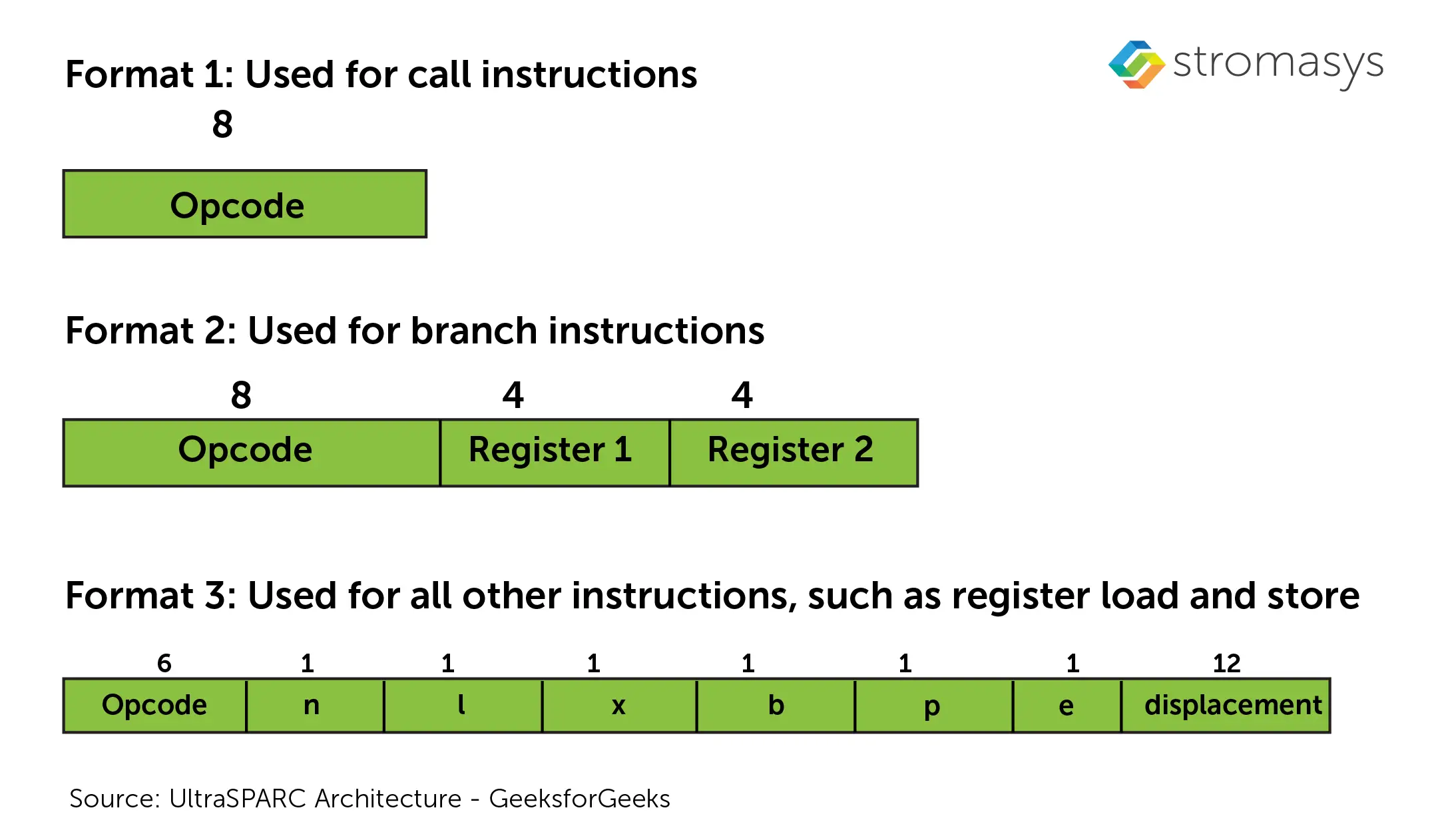
Now that you know the architecture, let’s look at the key architectures of the UltraSPARC series.
| Feature | UltraSPARC II | UltraSPARC III | UltraSPARC IV |
|---|---|---|---|
| Release Year | 1997 | 2001 | 2003 |
| Architecture | SPARC V9 (64-bit) | SPARC V9 (64-bit) | SPARC V9 (64-bit) |
| Clock Speed | 250 MHz to 650 MHz | 600-900 MHz | 1.05 GHz to 2.1 GHz |
| Core Count | Single | Single | Dual-core |
| Memory Bandwidth | 1.6 GB/s | 2.1 GB/s | 2.1 GB/s |
| Multithreading | Improved | Enhanced with multi-core support | Dual-core with improved multi-threading |
| Target Applications | High-performance servers and workstations | High-end servers, multi-threaded applications | High-end enterprise servers, databases |
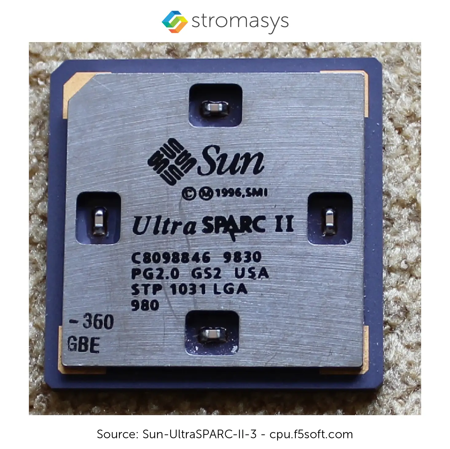
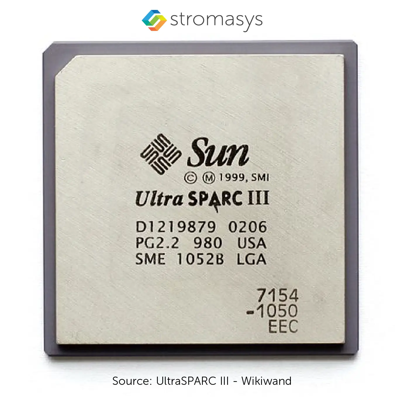
UltraSPARC III is an in-order superscalar microprocessor, meaning it responds to instructions in the order they are received and can issue multiple instructions per clock cycle.
It features an integrated memory controller and a dedicated multiprocessor bus to provide shared memory multiprocessing performance.
Additionally, it has the following noteworthy aspects:
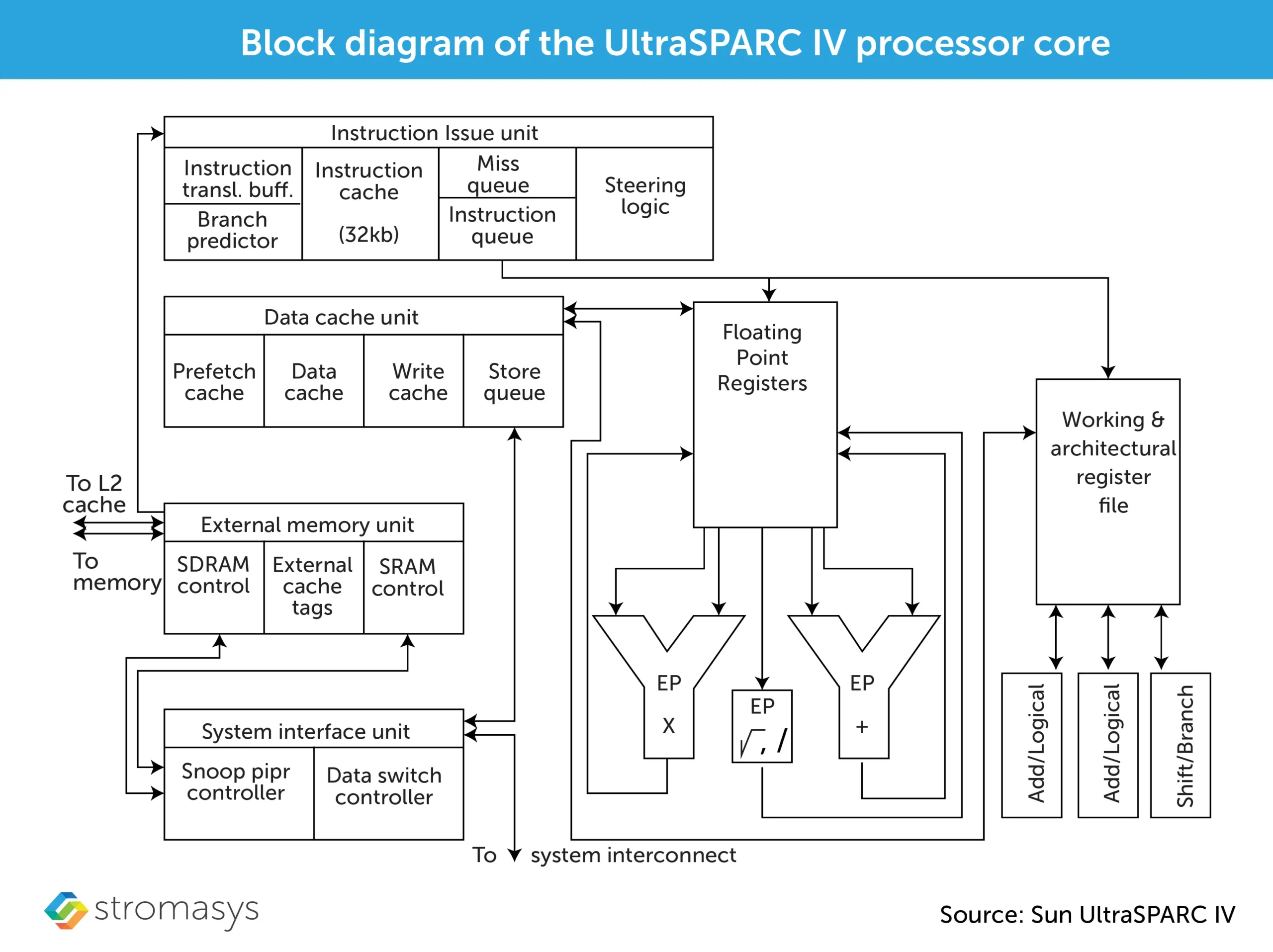
As part of the fourth generation of UltraSPARC microprocessors, it was the first multi-core SPARC processor. Sun’s Throughput Computing initiative led to the development of UltraSPARC IV.
Let’s take a look at the key characteristics of UltraSPARC IV:
Dual-core architecture: Features two UltraSPARC III-derived processor cores on a single chip.
Built in 0.13 µm CMOS: Fabricated using advanced technology with a clock frequency of 1.2 GHz.
Large cache system:
Cache operation:
Integer Execute Unit (IEU): Includes two add/logical units, a branch unit, and supports pipelined integer adds and multiplies.
Floating-Point Unit (FPU):
L2 Cache: 2×8 MB L2 cache, with 128 B cache lines (down from 512 B in UltraSPARC III) to reduce contention.
Memory Control Unit (MCU): On-chip MCU and the L2 cache controller to reduce latency.
Chip Multithreading (CMT): Each core executes one thread, a different form of multi-threading compared to traditional implementations.
Multi-processing support: Snoop controller ensures cache coherency across multi-processor systems.
Theoretical peak performance: 2.4 Gflop/s at 1.2 GHz.
Future scaling: Potential for frequency scaling in later stages of its lifecycle.
Chip Layout and Design: The Memory Control Unit and L2 cache controller are integrated into the chip to minimize latency.
The Sun4v architecture, introduced with the UltraSPARC T1 and T2 processors, brought built-in hypervisor support (Logical Domains / LDOMs). This enabled efficient hardware-level virtualization, allowing multiple Solaris instances to run on a single server with superior thread scalability and power efficiency. But with time and evolving technology, this SPARC server too started losing its value.
SPARC servers have their place in many organizations. Unfortunately, it’s not due to the uniqueness of the hardware anymore. Rather, it’s because they lack good alternatives for running their mission-critical Solaris applications.
These applications are vital to their business, powering day-to-day operations. But outdated hardware is causing serious issues: downtime, business disruption, security breaches, higher maintenance costs, spare parts scarcity, and a diminishing pool of skilled professionals.
This creates a situation that demands immediate action. Yet, businesses are either not prioritizing or don’t know where to start.
SPARC hardware emulation emerges as a risk-free, quick, and economical alternative here. If you’re looking for the leader in hardware emulation, Stromasys is the way to go.
Charon-SSP is Stromasys’ meticulously engineered SPARC emulator. It replicates the behavior of your current hardware and creates a similar environment on modern hardware, either on-premises or cloud.
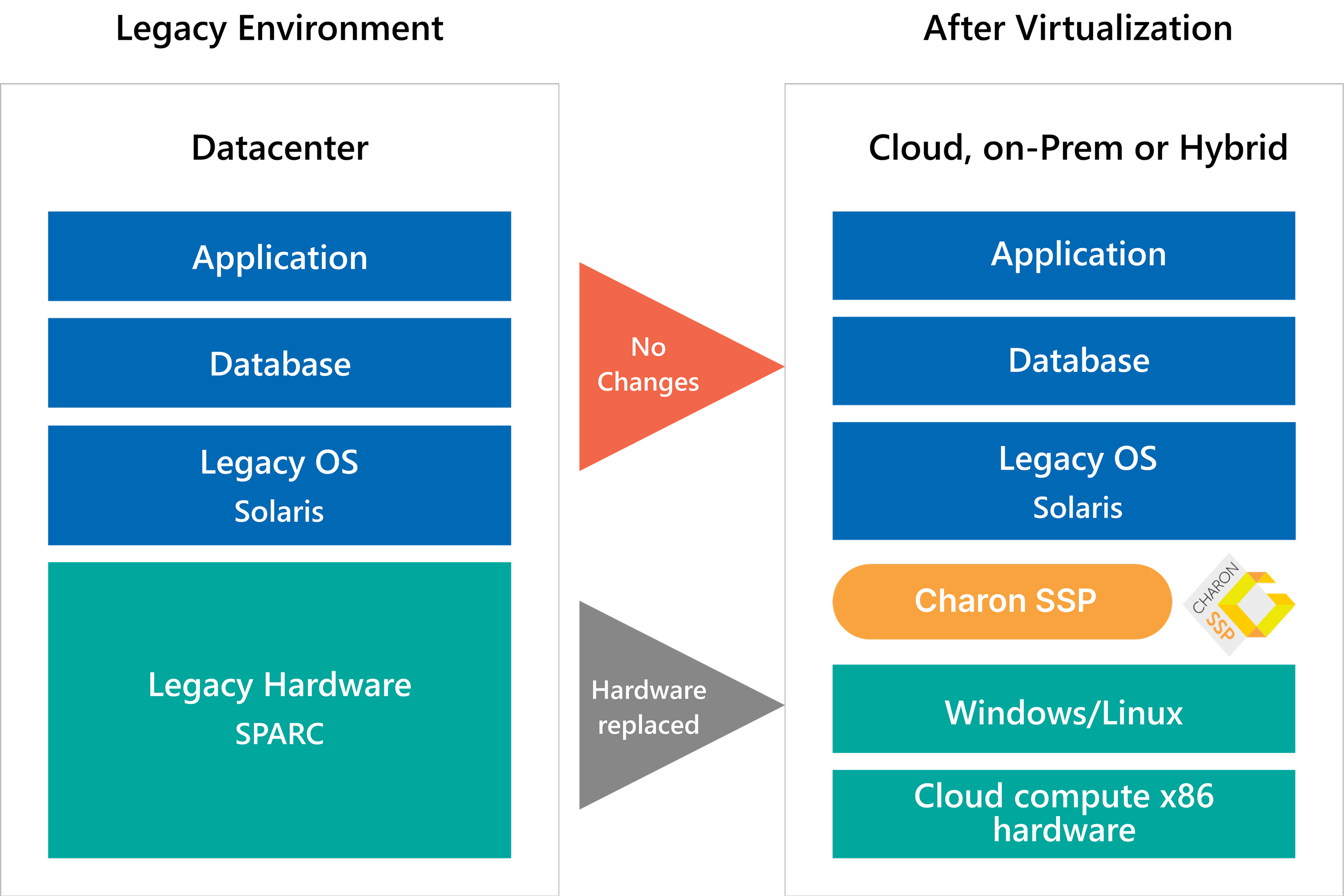
As a result, your critical legacy applications run unmodified on modern platforms without rewriting, re-designing, or recertifying. The entire process is frictionless and can be completed within days to weeks.
Discover how a risk-free
alternative to legacy migration extends the lifespan of your business applications.
The main difference between Pentium and UltraSPARC is that Pentium is based on CISC architecture whereas UltraSPARC is based on RISC architecture. UltraSPARC has a storage capacity of 8 MB while Pentium-4 has 256 KB.
UltraSPARC processors generally dominate the market for high-performance servers, workstations, and enterprise systems.
UltraSPARC processors are used predominantly under the Solaris operating system developed by Sun Microsystems.
Tuhin is a passionate writer with more than 7 years of experience in technical and marketing writing. With a unique ability to connect with his readers on a deeper level, he crafts content that not only captivates but also inspires action. Always on the cutting edge of industry trends, he excels at breaking down complex ideas into clear, engaging narratives that drive engagement and fuel business growth. Beyond his inherent inclination for writing, he is a sports enthusiast and a traveller, always seeking new experiences to enrich his perspective and creativity.
Companies still rely on mission-critical applications running on Sun SPARC, Alpha, or other legacy systems like PDP, VAX,...
Read MoreSPARC hardware has been trusted by companies around the world for decades now, and rightly...
Read MoreSun SPARC hardware was introduced in the late 1980s and was popular for its high-end...
Read MoreDon't let your legacy systems slow you down! Contact us today and transform your legacy environment into a dynamic, agile platform for success.
Kickstart your journey towards a more efficient and streamlined business environment with just one click.